Grey Havoc
ACCESS: USAP
- Joined
- 9 October 2009
- Messages
- 24,500
- Reaction score
- 18,175
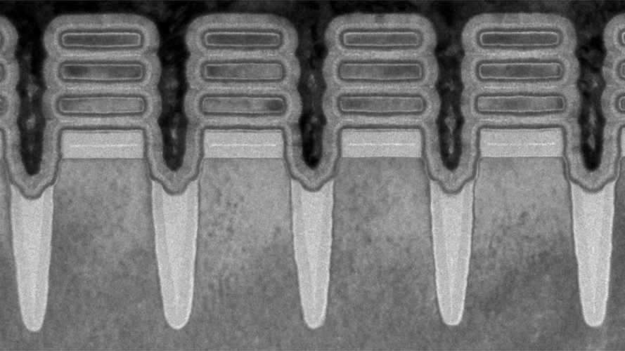
ORIGINAL CAPTION: Transistors on the IBM "nanosheet" it uses for the new tech
https://www.bbc.com/news/technology-57009930



The uploader has removed the video’s ability to be played on other websites.
Yeah, unfortunately you have to watch on YouTube. It's worth watching though, very good explanations.The uploader has removed the video’s ability to be played on other websites.
They've found a way to counter quantum tunneling. It's discussed in the video in post #6.Remind me, what's the chip size where QM starts really messing with your electron flow?
How much smaller can we make a classic transistor?
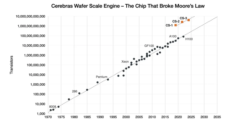
Disagree with the title on that chart, Cerebras is a large jump up (looks like a whole order of magnitude above the A100 chips) but it's still trending along per Moore's Law.
They don't do FP64 compute either apparently.Yes and the Cerebras processors are wafer-scale units. That’s been tried with varying levels of success by Intel, Cray, IBM, and DEC, among others. Viability of wafer-scale processors tends to depend on both manufacturing yield and the complexity of device-to-system interconnections.
The U.S. Defense Department has successfully, albeit surreptitiously, swiped $3.5 billion from the Commerce Department’s CHIPS Act funding to subsidize Intel’s creation of a classified advanced semiconductor manufacturing facility called Secure Enclave.
Well get this, the "2 nm" label is just marketing speak. There are no features on the chip of that size.I have to admit, the first time I read the title to this thread my first thought was "2 nautical miles, that seems kind of big"